Ceramic Substrate Series - Application of Laser Technology in Ceramic Substrate Field
Due to the inherent hardness and fragility of ceramic materials, the preparation of vias, shape cutting, or wafer dicing poses significant challenges. Traditional mechanical processing methods are time-consuming, labor-intensive, and can introduce stress, leading to potential damage to the ceramic substrate. Laser technology, as a flexible, efficient, and high-yield processing method, has demonstrated extraordinary capabilities in ceramic substrate processing.
1. Advantages of Laser Technology
Laser technology is an advanced processing technique that offers non-contact processing, no tool wear, high precision, and high flexibility. It has advantages such as high precision, efficient controllability, small heat-affected zone, no cutting force, and no "tool" wear, making it one of the most ideal means for ceramic processing.
1) The laser cutting head does not come into contact with the material surface, avoiding scratching the workpiece.
2) Narrow cutting gap, saving material.
3) The laser spot is small, with high energy density, high accuracy, fast speed, and high stability in line width and depth.
4) Laser processing is precise, resulting in smooth and burr-free cutting edges.
5) Small heat-affected zone, minimal local deformation of the workpiece, and no mechanical deformation.
6) Good processing flexibility, capable of processing any shape and cutting profiles.
2. Applications of Laser in Ceramic Substrates
Due to the large shrinkage during sintering, it is challenging to ensure the dimensional accuracy of ceramic pieces after sintering, including the precise provision of various holes, slots, and edges for assembly purposes. Therefore, post-sintering processing is required. Laser cutting, as a non-contact processing method, ensures that there is no internal stress in the product, resulting in minimal edge chipping, high precision, and high processing yield.
1) Laser scribing/cutting
Laser scribing, also known as scratch cutting or controlled fracture cutting, involves focusing the laser beam onto the ceramic substrate's surface through a beam delivery system. This generates heat, causing thermal ablation, melting, and vaporization of the ceramic in the scribed area, forming a series of blind holes or grooves on the ceramic surface. When stress is applied along the scribed line, material fracture occurs easily and accurately due to stress concentration, resulting in separation.
2) Laser scribing
In the scribing process of post-sintered ceramic substrates, lasers also find extensive applications. Scribing involves using a laser to burn continuous, densely arranged point-like pits on the ceramic surface, forming lines that facilitate the division of the substrate into individual units after packaging.
3) Laser drilling
Drilling is the most commonly used laser processing technique in the production of HTCC (High-Temperature Co-Fired Ceramic), LTCC (Low-Temperature Co-Fired Ceramic), and DPC (Direct Plated Copper) substrates. A laser drilling machine is used to create holes that connect the upper and lower surfaces of the substrate, serving as paths for vertical interconnection. This enables three-dimensional packaging and integration of electronic devices on ceramic substrates.
Different types of ceramic materials require specific laser beams, such as infrared, green light, ultraviolet, or CO2 lasers, to irradiate the material surface. Each laser pulse burns off a portion of the material. Laser drilling offers several advantages compared to mechanical drilling, including higher processing precision, lower consumable costs, and increased product flexibility.
4) Laser marking
Laser marking involves using a laser marking machine to engrave product QR codes onto ceramic substrates. Laser marking is a widely used laser processing technique that utilizes high-energy density lasers to locally irradiate the workpiece, causing vaporization or color change in the surface material, thus creating permanent markings.
With the continuous development of the microelectronics industry, electronic components are gradually moving towards miniaturization and lightweight design. The demand for precision is also increasing. This inevitably imposes higher requirements on the processing of ceramic substrates, making laser technology highly promising.
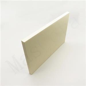
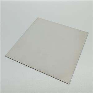
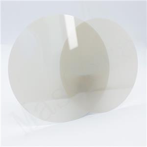
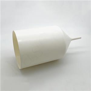
Mascera produces high-quality ceramic substrates using alumina, aluminum nitride, and silicon nitride as materials, and has introduced laser equipment on the production line for laser cutting, scribing, and drilling according to customer requirements. The size accuracy is high, the processing speed is fast, and the product stability is good. For surface treatment, polishing or DPC&DBC metallization can also be provided. If you want our quotation, please send us your design or requirement details.


