Silicon Carbide Ceramics: Precision Components Essential for Semiconductor Processes (Part 2)
Lithography Process
• Silicon Carbide Wafer Chuck, Ceramic Square Mirror, Photomask Films
SiC Wafer Chuck, Ceramic Square Mirror, Photomask Films Lithography primarily focuses on exposing circuit patterns onto silicon wafers using optical systems. The precision of this process directly affects the performance and yield of integrated circuits. As one of the top-tier devices in chip manufacturing, lithography machines contain up to hundreds of thousands of components. Both the optical elements and components within the lithography system require extreme precision to ensure circuit performance and accuracy. SiC ceramics find applications in wafer chucks and ceramic square mirrors.

Lithography Machine Structure
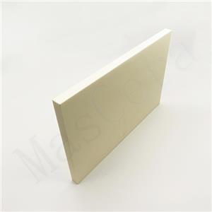
Wafer Chuck
The wafer chuck in lithography machines bears and moves wafers during exposure. Precise alignment between the wafer and chuck is essential for accurate replication of patterns onto the wafer surface. SiC wafer chucks, known for their lightweight nature, high dimensional stability, and low thermal expansion coefficients, reduce inertial loads, improve motion efficiency, positioning accuracy, and stability.

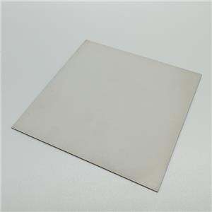
Ceramic Square Mirror
Synchronization of motion between the wafer chuck and mask stage is crucial in lithography machines, directly influencing lithography precision and yield. The square mirror, a crucial part of the feedback measurement system for the scanning and positioning of the wafer chuck, demands lightweight materials with stringent requirements. While SiC ceramics possess the desired lightweight characteristics, manufacturing such components is challenging. Currently, leading international integrated circuit equipment manufacturers predominantly use materials like fused silica and cordierite.
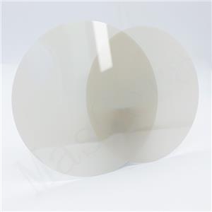
However, advancements in technology have led Chinese experts to achieve the fabrication of large-sized, complex-shaped, highly lightweight, fully enclosed SiC ceramic square mirrors, and other functional optical components for lithography machines.Photomask Films Photomasks, also known as reticles, transmit light through masks to form patterns on photosensitive materials. However, when EUV light irradiates photomasks, heat is emitted, raising temperatures to between 600 and 1,000 degrees Celsius, potentially causing thermal damage. Therefore, a layer of SiC film is typically deposited on photomasks. Many foreign companies, such as ASML, now supply films with over 90% transmittance to reduce cleaning and inspection during photomask use, enhancing efficiency and product yield of EUV lithography machines.
Plasma Etching and Deposition
The photomask, also known as a reticle, primarily functions to transmit light through a mask and form patterns on photosensitive materials. However, when EUV (Extreme Ultraviolet) light irradiates the photomask, it emits heat, raising temperatures to between 600 to 1,000 degrees Celsius, potentially causing thermal damage. Therefore, it's common to deposit a layer of silicon carbide (SiC) film on the photomask to mitigate this issue. Currently, many foreign companies, such as ASML, have begun supplying films with over 90% transparency to reduce the need for cleaning and inspection during photomask use, thereby improving the efficiency and product yield of EUV lithography machines.

Plasma Etching and Deposition
• Focus Rings and Others
In semiconductor manufacturing, the etching process utilizes liquid or gaseous etchants (such as fluorine-containing gases) ionized into plasma to bombard wafers, selectively removing undesired materials until the desired circuit patterns remain on the wafer surface. Conversely, film deposition is akin to the reverse of etching, utilizing deposition methods to stack insulating materials between metal layers, forming thin films. As both processes employ plasma technology, they are prone to corrosive effects on chamber and components. Therefore, components inside the equipment require good plasma resistance, low reactivity to fluorine etching gases, and low conductivity.
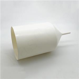
Traditional etching and deposition equipment components (such as focus rings) are typically made from materials like silicon or quartz. However, with the advancement of integrated circuit miniaturization, the demand and importance of etching processes in IC manufacturing continue to increase. High-energy plasma is needed for precise silicon wafer etching at the microscopic level, enabling smaller linewidths and more complex device structures. Consequently, chemical vapor deposition (CVD) silicon carbide (SiC) has gradually become the preferred coating material for etching and deposition equipment due to its excellent physical and chemical properties, high purity, and uniformity. Currently, CVD silicon carbide components in etching equipment include focus rings, gas showerheads, trays, and edge rings. In deposition equipment, there are chamber lids, chamber liners, and SiC-coated graphite baseplates.


Focus Rings, SiC-Coated Graphite Baseplates
Due to the low reactivity and conductivity of CVD silicon carbide to chlorine and fluorine etching gases, it has become the ideal material for components like focus rings in plasma etching equipment. CVD silicon carbide components in etching equipment include focus rings, gas showerheads, trays, edge rings, and more. Taking focus rings as an example, they are crucial components placed outside the wafer and directly in contact with it. By applying voltage to the ring, plasma passing through the ring is focused onto the wafer, improving processing uniformity. Traditionally, focus rings were made of silicon or quartz. However, with the advancement of integrated circuit miniaturization, the demand and importance of etching processes in IC manufacturing continue to increase. Plasma etching power and energy requirements continue to rise, especially in capacitively coupled plasma (CCP) etching equipment where higher plasma energy is needed. As a result, the usage of focus rings made from silicon carbide material is increasing.
XIAMEN MASCERA TECHNOLOGY CO., LTD. is a reputable and reliable supplier specializing in manufacturing and sales of technical ceramic parts. We provide custom production and high precision machining for a wide series of high performance ceramic materials including alumina ceramic, zirconia ceramic, silicon nitride, silicon carbide, boron nitride, aluminum nitride and machinable glass ceramic. Currently, our ceramic parts can be found in many industries like mechanical, chemical, medical, semiconductor, vehicle, electronic, metallurgy etc. Our mission is to provide the best quality ceramic parts for global users and it is a big pleasure to see our ceramic parts work efficiently in customers' specific applications. We can cooperate on both prototype and mass production, welcome to contact us if you have demands.