Applications and Advantages of Ceramic Vacuum Chucks vs. Electrostatic Chucks
In semiconductor manufacturing and precision processing, technical ceramics play a crucial role in ensuring high-precision wafer handling. Two widely used ceramic-based clamping technologies are ceramic vacuum chucks and ceramic electrostatic chucks. These chucks utilize alumina ceramic or porous ceramic to provide exceptional mechanical stability, chemical resistance, and thermal performance, making them ideal for handling delicate wafers and substrates.
This article explores the differences between ceramic vacuum chucks and electrostatic chucks, their respective working principles, and their applications in semiconductor fabrication and precision industries.
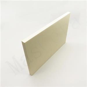
Ceramic Vacuum Chucks
Ceramic vacuum chucks use negative pressure (vacuum suction) to securely hold wafers, substrates, or other precision components. These chucks typically incorporate porous ceramic surfaces, enabling uniform vacuum distribution and ensuring firm adhesion without mechanical stress.
Features of Ceramic Vacuum Chucks
● Material Composition
Most vacuum chucks use high-purity alumina ceramic for its hardness, low thermal expansion, and excellent wear resistance.
● Porous Surface Design
Porous ceramic structures allow for uniform vacuum distribution, preventing damage to sensitive materials.
● Flatness and Stability
Designed to maintain wafer planarity, minimizing defects and improving process yield.
● Non-Contact Handling
Reduces contamination risks compared to mechanical clamping methods.
● Customization
Available in different pore sizes and vacuum channel designs to suit diverse industrial needs.
Applications of Ceramic Vacuum Chucks
● Wafer Processing:Used in semiconductor lithography, metrology, and dicing.
● Optical and Display Panel Manufacturing: Ensures stability for thin-film deposition.
● Microelectronics and MEMS Fabrication: Essential for handling fragile substrates during assembly and inspection.
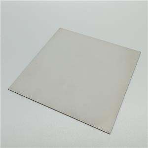
Ceramic Electrostatic Chucks
Ceramic electrostatic chucks (ESCs) use electrostatic forces to attract and hold wafers, rather than relying on vacuum suction. ESCs consist of a technical ceramic dielectric layer with embedded electrodes that generate an electrostatic field when voltage is applied.
Features of Ceramic Electrostatic Chucks
● Ceramic as Dielectric
Ensures excellent electrical insulation and high-temperature resistance.
● Non-Contact Clamping
Reduces the risk of wafer warpage or deformation.
● Stable Holding in Vacuum
Unlike ceramic vacuum chucks, ESCs work efficiently in low-pressure environments.
● Enhanced Thermal Control
Many ESCs incorporate helium backside gas cooling for improved wafer temperature regulation.
● Bipolar and Monopolar Configurations
Bipolar designs offer more uniform clamping force, while monopolar designs provide simpler operation.
Applications of Ceramic Electrostatic Chucks
● Plasma Etching and CVD: Used in vacuum chambers where traditional ceramic vacuum chucks cannot function.
● Ion Implantation: Provides stable wafer retention during high-energy processes.
● Semiconductor Manufacturing: Supports 300mm and 200mm wafers in high-precision fabrication.
● Advanced Packaging and MEMS Production: Ensures minimal particle contamination and high-precision positioning.
Comparison: Vacuum Chucks vs. Electrostatic Chucks
| Feature | Vacuum Chucks | Electrostatic Chucks |
| Clamping Method | Vacuum suction | Electrostatic force |
Material | Porous ceramic (Alumina) | Technical ceramics (Alumina, AlN) |
| Use in Vacuum | Not suitable for high-vacuum environments | Ideal for vacuum chambers |
| Thermal Management | Passive (relies on chuck material properties) | Active (uses helium backside gas cooling) |
| Applications | Lithography, wafer dicing, inspection | Plasma etching, CVD, ion implantation |
Both ceramic vacuum chucks and alumina electrostatic chucks are essential in precision manufacturing and semiconductor fabrication. While vacuum chucks offer simplicity and effective wafer clamping in ambient environments, electrostatic chucks provide superior performance in vacuum processes and enable advanced thermal management.
By leveraging technical ceramics, manufacturers can achieve high precision, reliability, and contamination-free handling, ensuring high yields in semiconductor and electronics production. Choosing the right chuck depends on process requirements, environmental conditions, and wafer handling needs.